The record for the largest chip size may sound dubious, but not in the case of TSMC. The company introduced the Chip-on-Wafer-on-Substrate (CoWoS) packaging technology, which will allow for System-in-Package (SiP) systems that are many times larger than existing NVIDIA B200 or AMD Instinct MI300X processors. The processors will have monstrous dimensions of 120 x 120 mm and will consume kilowatts of energy.
"CoWoS®, SoIC, and System-on-Wafer (TSMC-SoW™): TSMC's Chip-on-Wafer-on-Substrate (CoWoS) has become a key factor in the artificial intelligence revolution, allowing customers to use more processor cores and high-bandwidth memory (HBM) stacked side by side on a single intermediate device. At the same time, our System-on-Integrated Chips (SoIC) has proven to be the leading solution for stacking 3D chips, and customers are increasingly combining CoWoS with SoIC and other components for maximum system integration into a package (SiP).
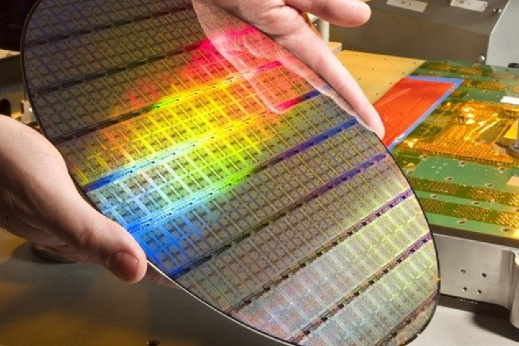
Thanks to the System-on-Wafer, TSMC offers a new revolutionary option that allows the use of a large array of matrices on a 300mm plate, offering greater computing power, occupying much less space in the data processing center, and increasing performance per watt by orders of magnitude. The first TSMC SoW offering, a plate with logical circuitry based on Integrated Fan-Out technology (InFO), is already in production. The chip-on-wafer version using CoWoS technology is scheduled for 2027, which will allow the integration of SoIC, HBM, and other components to create a powerful plate-level system with computing power comparable to a server rack data processing center or even a whole server."
The platform uses the previously developed InFO_SoW technology by the company, allowing for the creation of large-sized chips, as well as the System-on-Integrated Chips (SoIC) technology. Another technology, Chip-on-Wafer (CoW), allows for placing memory or other elements on top of the system.
In fact, we are talking about processors comparable in size to a whole 300mm silicon plate, which will allow for a huge number of cores to be accommodated. This packaging method for cores will enhance performance and energy efficiency through high speeds between components. Inside, the system will have low latency between cores and low resistance in energy transfer. Unlike previous technologies, CoWoS allows for the use of different process technologies and high-speed HBM4 memory in chip layout.
Sources: TSMC, Tom's Hardware


Comments (0)
There are no comments for now