


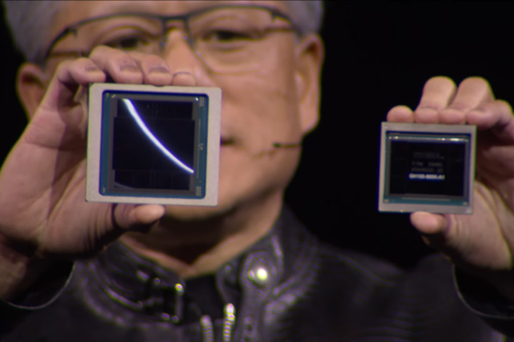
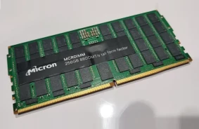
During the GTC March 2024 Keynote, NVIDIA introduced the Blackwell chip architecture and the B200 graphics processors based on it. The new GPUs with AI capabilities will replace the H100 and H200 data processing centers. The Blackwell Blackwell GB200 chips will combine the Grace architecture with the Blackwell architecture.
The B200 graphics processor contains 208 billion transistors (compared to 80 billion on the H100/H200). It provides 20 petaflops of AI performance from a single GPU - one H100 had a maximum of 4 petaflops in AI calculations. The chips will receive 192 GB of HBM3e memory, which provides up to 8 TB/s bandwidth.
The Blackwell B200 is not a traditional GPU in the ordinary understanding. It consists of two closely connected crystals that function as a unified CUDA graphics processor. Two chips are connected by the NV-HBI (NVIDIA High Bandwidth Interface) with a speed of 10 TB/s.
The Blackwell B200 is manufactured using the TSMC 4NP process, an enhanced 4N compared to the Hopper H100 and Ada Lovelace. The process does not offer a significant improvement in density, so making the chip larger was necessary to increase computational power, which can explain the combination.
Each crystal has four stacks of 24 GB HMB3e each with a bandwidth of 1 TB/s on a 1024-bit interface. For comparison, the H100 had six stacks of 16 GB HBM3. The 20 petaflops performance of the Blackwell B200 is achieved through a new FP4 number format with double the bandwidth compared to the FP8 format of the Hopper H100.
NVIDIA Blackwell Chip Options
The largest and fastest solution will be the GB200 superchip, which consists of two B200 GPUs. This "monster" has a customizable TDP of up to 2700 W - for two chips (four GPUs) plus one Grace processor. Values up to 20 petaflops FP4 for one B200 - are taken for half of the GB200 superchip. It is not specified what the TDP is for a single B200 GPU.
Another Blackwell option is the HGX B200, which is based on using eight B200 GPUs with an x86 processor in one server node. They are configured for 1000 W per B200, and the GPUs provide up to 18 petaflops bandwidth FP4 – 10% slower than the GB200.
There will also be the HGX B100 chip. The same basic design as the HGX B200, with an x86 processor and eight B100 GPUs, but designed for compatibility with existing HGX H100 infrastructure and provides the fastest deployment. TDP for the GPU is limited to 700 W, like in the H100, and the bandwidth drops to 14 petaflops FP4 per GPU. All three of these configurations have the same 8 TB/s bandwidth per GPU.
NVIDIA NVLINK 7.2T
For communication between multiple NVIDIA nodes, the company introduces the fifth-generation NVLink chips and NVLink Switch 7.2T. The new NVSwitch chip has a bidirectional bandwidth of 1.8 TB/s. This chip with 50 billion transistors is also manufactured using the TSMC 4NP process.
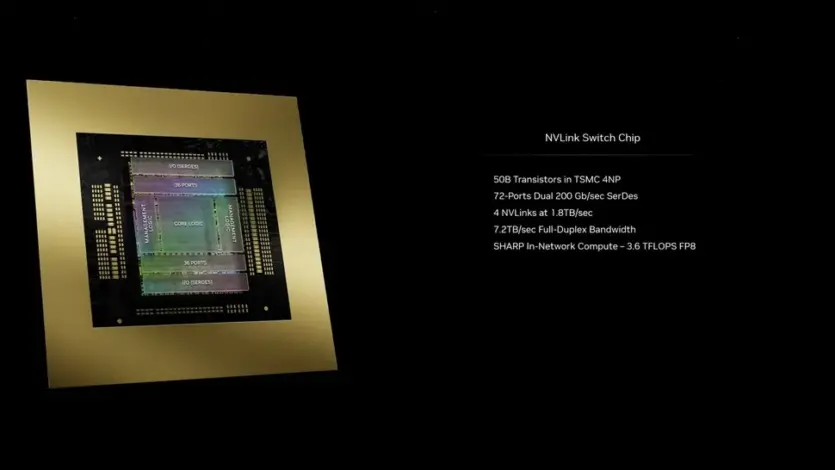


The connector processor almost reaches the size of the Hopper H100, demonstrating the importance of connectivity following the increase in computing power and data speed. The previous generation supported up to 100 GB/s bandwidth. The new NVSwitch provides an 18-fold acceleration compared to the multi-node connectivity of the H100.
Each Blackwell graphics processor is equipped with 18 fifth-generation NVLink connections. This is eighteen times more than was available for the H100. Each connection offers 50 GB/s bidirectional bandwidth, or 100 GB/s per connection. With such speed, large groups of GPU nodes can operate as if they were just one massive GPU.
NVIDIA B200 NVL72
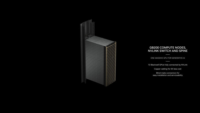
The new chips with the new interface are combined into NVIDIA B200 NVL72 servers. Essentially, this is a full rack solution with 18 1U servers, each of which has two GB200 superchips. Two B200 GPUs are paired with one Grace CPU, whereas the GH100 technology used a smaller solution - one Grace CPU next to one H100 GPU.


Each computational node in the GB200 NVL72 has two GB200 superchips, so one tray contains two Grace processors and four B200 GPUs with 80 petaflops FP4 AI and 40 petaflops FP8 AI. These are 1U servers with liquid cooling that take up a significant portion of the standard 42U rack space.
In addition to the computational panels of the GB200 superchips, the GB200 NVL72 will also have NVLink switch panels. These are also 1U trays with liquid cooling, with two NVLink switches per tray and nine such trays per rack. Each tray provides 14.4 TB/s of total bandwidth.
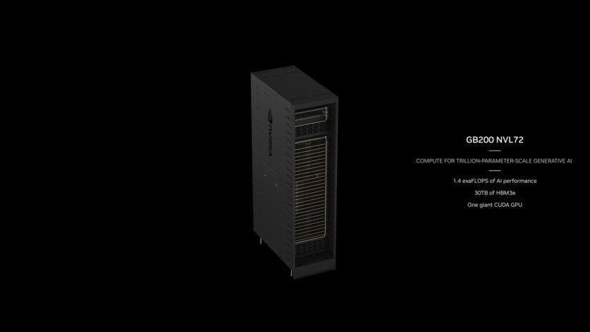
Overall, the GB200 NVL72 has 36 Grace processors and 72 Blackwell GPUs with 720 petaflops FP8 and 1440 petaflops FP4. With the available 130 TB/s multi-node bandwidth, NVL72 can process up to 27 trillion AI speech model parameters. The remaining racks are intended for networks and other elements of the data processing center.
Also presented are SuperPOD supercomputers that combine multiple GB200. Currently, NVLink supports up to 576 GPU domains, and the new DGX SuperPOD scales precisely to this number of GB200 Blackwell GPUs. Each SuperPOD can accommodate up to eight GB200 NVL72 systems, equivalent to 288 Grace processors and 576 B200 GPUs.
Source: Tom's Hardware


Comments (0)
There are no comments for now